 2025/12/05
Background knowledge
In the semiconductor industry's "micron-scale battlefield," the packaging process serves as the critical hub connecting chips to external circuits, directly determining their performance stability and lifespan. Copper pads, with their exceptional thermal and electrical conductivity, become the core components in key connections such as "chip-substrate" and "substrate-heat sink" interfaces. The flatness of copper pads is even more crucial, acting as the "invisible lifeline" that affects packaging yield—any micron-scale protrusion or depression may lead to poor solder joints, heat dissipation failures, and ultimately chip failures.
Traditional flatness measurement methods, plagued by insufficient precision and low efficiency, fail to meet the semiconductor industry's dual demands for "high precision and high throughput." In this context, 3D industrial cameras have emerged as the "core solution" for semiconductor copper pad flatness inspection, leveraging their nanometer-level measurement accuracy and high-speed detection capabilities to fortify the quality control of semiconductor packaging.

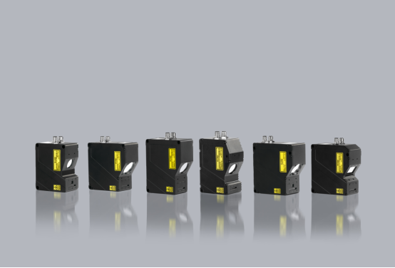
Camera Selection
Today, we're excited to showcase the LVM3415 linear laser 3D camera, a new addition to Next Vision Tech's LVM3400 series, and its real-world applications in the consumer electronics industry!
The LVM3415 3D intelligent sensor features a full-frame acquisition rate of 2000Hz, with ROI settings capable of reaching up to 30000Hz. It effortlessly handles high-speed dynamic scenes, delivering repeatable precision of 0.3μm and capturing every detail, thus meeting the demands of high-precision industrial inspection.
surveillance project
Measure product flatness
·Crafted from brass with a diffuse reflective surface (no high-gloss), measuring approximately 15mm in diameter.
·Repeatability: 0.05mm
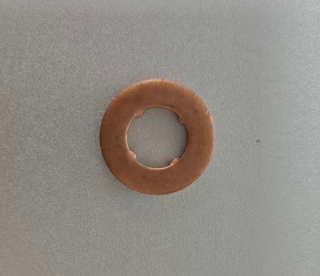
Product image
Detection environment and installation method
·Scanning method: The camera is fixed in place, and the test specimen is scanned along a central linear path for measurement.
·Triggering method: Encoders are used for triggering to output stable AB phase difference signals
·Communication method: TCP/IP Ethernet
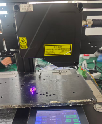
Image capture effect
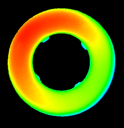
*The image shows the product in detail
measured data
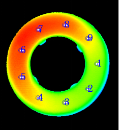
·Depth image acquired by camera
Place 9 ROI fitting planes on the product surface to calculate its planarity.
·Collect images continuously for 10 times and calculate the flatness repeatability data
DA
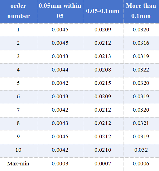
*10 static measurements, maximum repeatability of 0.0007mm for 3 products across 10 repetitions
Test conclusion
This solution delivers comprehensive imaging results with sharp feature images. The LVM3415 camera enables precise flatness measurement of products, achieving detection accuracy within 0.005mm to meet customer requirements.
·Speed: The camera can scan at a maximum speed of 66mm/s
The camera's focal length ranges from 18mm to 21mm, providing full coverage of the product.

